HOME > シリコン Silicon
シリコン Silicon
半導体材料の代名詞としてのシリコン。
シリコン(Si,silicon、ケイ素)は、
- 資源が豊富。(地球上で酸素の次に多く存在する元素)
- 高純度化し易く硬くて丈夫。
- 安定した酸化膜が形成出来、高集積化し易い。
- 結晶を大型化し易い。
等の理由で、半導体材料として幅広い分野で使用されています。
1998年の創業当初より、中国製のSi(シリコン)に着目し、2003年には、国内大手パワーデバイスメーカーに、中国製シリコン素材としては、国内初の量産プライム材料としての正式認定を得ました。
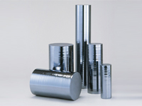
Φ2インチ~Φ6インチまでのパワーデバイス用プライムウェハーの製造を中心に、構造用部品材料としてΦ450mmまでの単結晶大口径シリコンインゴット・プレートの供給と加工も行っております。
Strong point of Si (Silicon) as synonymous with the semiconductor material.
- Abundant resources. (existing element a lot of on the earth next to oxygen)
- It is easy to become high purity and is hard and strong.
- We can form a stable oxidation film and are easy to become high integration.
- It is easy to make a big size crystal.
We pay our attention to Chinese Si (silicon) material since we started our business in 1998,
got the official authorization of the domestic major power device maker as mass production prime materials in 2003.
It was the domestic first achievement by Chinese silicon materials.
Our main products is the prime wafer from 2inches to 6inches for power devices.
We can supply and process the large-dia.(Max.φ450mm) Silicon ingot and plate for a part for various mechanism,too.
 |
 |
 |
インゴット・ウェハー Ingot・Wafer
供給可能なシリコン素材
**画面より大きな表はスクロール可能です
| Growth Method | Type | Orientation | Diamater(mm) | Resistivity(Ω・cm) |
|---|---|---|---|---|
| CZ | P,N | <100><111><110> | 50 - 450 | 1 - 300 |
| MCZ | P,N | <100><111><110> | 76.2 - 450 | 1 - 300 |
| CZ(Heavily Doped) | P,N | <100><111> | 50 - 200 | 0.001 - 1 |
| FZ | P,N | <100><111><110> | 50 - 150 | > 100 |
| NTDFZ | N | <100><111><110> | 76.2 - 150 | 30 - 800 |
| CFZ | P,N | <100><111><110> | 76.2 - 150 | 1 - 50 |
| GDFZ | P,N | <100><111><110> | 76.2 - 150 | 0.001 - 150 |
シリコン特性データ
基本特性 |
化学組成 |
Si |
|---|---|---|
機械特性 |
比重 |
2.329(25℃) |
熱特性 |
融点 |
1,420℃ |
光学特性 |
反射損失 |
46.1%(10μ)
1.2~15.0 |
電気特性 |
体積固有抵抗 |
2.4×10⁴Ω・cm(25℃) |
シリコンエピタキシャルウェハー Silicon Epitaxal Wafer
Φ8inchまでの各種Si Epi wafer を供給いたします。
Maximum size : ~Φ8 inch.
Silicon Epitaxial Wafer Specifications
**画面より大きな表はスクロール可能です
| Item | Characteristics | Parameters | Test Method | ||||
|---|---|---|---|---|---|---|---|
| 1 | Epitaxial Layer Dopants | Boron,Phosphorus,Arsenic | |||||
| 2 | Crystal Orientation in the Epitaxial Layer | <100>,<111> | |||||
| 3 | Epitaxial Layer Resistivity | Epitaxial Reactor |
Diameter | Type | Epitaxial Wafer Resistivity | Uniformity | ASTM F723 F1392 |
| Batch | 100mm 125mm 150mm 200mm |
P/P++;N/N+ N/N++;N/N+/N++ N/P/P;P/N/N+ |
0.004 (B:0.01) -3 Ω.cm | ≤±3% | |||
| 3-30 Ω.cm | ≤±5% | ||||||
| >30 Ω.cm | ≤±6% | ||||||
| Single | 150mm 200mm |
P/P++;N/N++ N/N+/N++ |
0.3-3 Ω.cm | ≤±2% | |||
| 3-30Ω.cm | ≤±3% | ||||||
| 4 | Epitaxial Layer Thickness | Epitaxial Reactor |
Diameter | Type | Epitaxial Wafer Resistivity | Uniformity | ASTM F95 |
| Batch | 100mm 125mm 150mm 200mm |
P/P++;N/N+ N/N++,N/N+/N++ N/P/P;P/N/N+ |
3-100um | ≤±3% | |||
| Single | 150mm 200mm |
P/P++;N/N++ N/N+/N++ |
0.1-20um | ≤±1% | |||
| 5 | Stacking faults density | ≤10cm2 | ASTM F1810 | ||||
| 6 | Slip lines | ≤5 lines,total length<1/2 diameter | ASTM F1725 F1726 |
||||
| 7 | Haze,Scratches,Craters,Orange peel,Cracks,Crow's feet,Edge chips, Foreign matter,Back surface contamination | NONE | ASTM F523 | ||||
| 8 | Crown edge | Projection above wafer surface not to exceed 1/3 of Epitaxial layer thickness | |||||
| 9 | Point defects | SEMI Standard | ASTM F523 | ||||
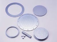
パーツ Parts
スライス、ラッピング、エッチング、ポリッシングからマシニング加工、微細加工まで各種精密加工承ります。
We can accept all kinds of processing (Slicing , Lapping , Etching , Polishing , Machining and Minute Process) .